Mastering Footprint Creation and Management in Autodesk Electrical: A Comprehensive Guide
James June 7, 2024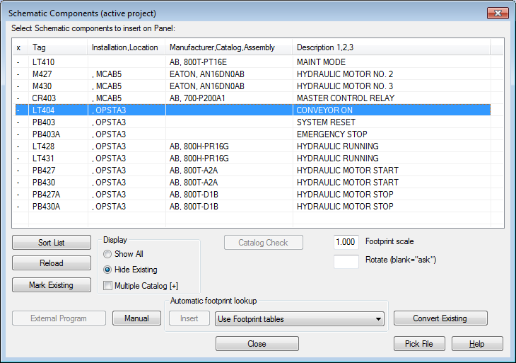
Footprints are essential elements in electrical design, serving as representations of physical components on printed circuit boards (PCBs). In Autodesk Electrical, creating and managing footprints is crucial for accurately placing components on PCB layouts and ensuring compatibility with manufacturing processes. In this comprehensive guide, we will delve into the intricacies of creating and managing footprints in Autodesk Electrical, providing detailed instructions, best practices, and expert tips to help you master this critical aspect of PCB design.
Understanding the Significance of Footprints
Footprints, also known as land patterns or decals, are geometric representations of electronic components’ physical dimensions and mounting configurations on PCBs. The significance of footprints in PCB design encompasses several key areas:
- Component Placement: Footprints guide the placement of electronic components on PCB layouts, ensuring proper alignment and orientation for soldering and assembly.
- Manufacturability: Accurate footprints facilitate seamless integration with manufacturing processes such as pick-and-place assembly, solder paste deposition, and reflow soldering.
- Signal Integrity: Properly designed footprints optimize signal integrity and minimize electromagnetic interference (EMI) by maintaining appropriate trace lengths, widths, and spacing.
Creating Footprints in Autodesk Electrical
Now, let’s explore the step-by-step process of creating footprints within Autodesk Electrical:
Step 1: Access Footprint Editor
- Footprint Manager: Navigate to the footprint manager or editor tool within Autodesk Electrical to access the interface for creating and managing footprints.
- Library Selection: Choose the desired footprint library or category containing predefined footprint templates.
Step 2: Define Footprint Dimensions
- Component Specifications: Gather detailed specifications and dimensions for the electronic component for which you are creating the footprint.
- Footprint Editor Tools: Utilize the footprint editor tools to define the outline, pad locations, and mounting holes of the footprint based on the component specifications.
Step 3: Configure Pad Layout
- Pad Placement: Position pads within the footprint to correspond with the component’s terminal locations and lead configurations.
- Pad Properties: Specify pad properties such as size, shape, spacing, and solder mask clearance to meet PCB fabrication and assembly requirements.
Step 4: Add Silkscreen and Assembly Details
- Silkscreen Markings: Include silkscreen markings, reference designators, and component outlines on the footprint for assembly and identification purposes.
- Assembly Features: Incorporate assembly features such as fiducial marks, polarity indicators, and component orientation markers to facilitate automated assembly processes.
Step 5: Validate and Save Footprint
- Validation Checks: Perform validation checks to ensure that the footprint dimensions, pad layouts, and assembly details adhere to design rules and manufacturing guidelines.
- Save and Store: Save the footprint to the designated library or repository for future use, ensuring accessibility and standardization across design projects.
Managing Footprints in Autodesk Electrical
In addition to creating footprints, it’s essential to manage them effectively within Autodesk Electrical:
Footprint Library Organization
- Library Structure: Organize the footprint library into categories, subcategories, and folders to facilitate easy navigation and retrieval.
- Naming Conventions: Adopt consistent naming conventions for footprints to ensure clarity, searchability, and standardization across design projects.
Version Control and Revision Management
- Versioning System: Implement a version control system to track changes and revisions to footprints over time.
- Revision History: Maintain a comprehensive revision history for each footprint, documenting the date, author, and nature of each revision.
Collaboration and Collaboration
- Team Collaboration: Foster collaboration among design team members, engineers, and manufacturers to gather feedback, share insights, and refine footprints collaboratively.
- Documentation and Documentation: Document footprint specifications, design considerations, and manufacturing requirements comprehensively for future reference and auditing purposes.
Best Practices for Footprint Creation and Management
To optimize the process of footprint creation and management in Autodesk Electrical, consider the following best practices:
Component Verification and Validation
- Datasheet Reference: Refer to component datasheets and manufacturer specifications to ensure accurate footprint creation.
- Prototype Testing: Prototype PCB assemblies to validate footprint compatibility and functionality before full-scale production.
Standardization and Standardization
- Standard Library: Establish a standardized library of footprints comprising commonly used components to ensure consistency and compatibility across design projects.
- IPC Standards: Adhere to industry standards such as those defined by the Institute for Interconnecting and Packaging Electronic Circuits (IPC) for footprint design and documentation.
Continuous Improvement and Improvement
- Feedback Mechanism: Solicit feedback from PCB fabricators, assemblers, and end-users to identify areas for improvement in footprint design and functionality.
- Continuous Learning: Stay updated on emerging technologies, materials, and manufacturing processes to incorporate the latest advancements into footprint design practices.
Conclusion
Creating and managing footprints in Autodesk Electrical is a fundamental aspect of PCB design, enabling accurate component placement, seamless integration with manufacturing processes, and optimal signal integrity. By following the steps outlined in this guide and adhering to best practices, you can master the footprint creation and management process, streamline PCB design workflows, and enhance collaboration and communication among design team members and stakeholders. Whether you’re designing PCBs for consumer electronics, industrial automation, or telecommunications applications, proficiency in footprint creation and management will empower you to deliver superior results and exceed client expectations.